 Place your first PCB order without fully understanding the process, and there is a good chance you will receive a blank, copper-traced board with no components fitted, and wonder where everything went wrong.
It is one of the most common sources of confusion in electronics procurement. PCB fabrication and PCB assembly are not two names for the same thing. They are two entirely separate stages in the production of a working electronic circuit, each requiring different equipment, different expertise, different input files, and different quality standards.
Getting them confused does not just cause a moment of embarrassment. It leads to misaligned supplier briefs, incorrect cost estimates, missed lead times, and in the worst cases, production errors that are expensive to unpick.
This article explains what each stage involves, how they connect within a real product development lifecycle, and what engineers and procurement professionals in high-reliability sectors need to consider when choosing a manufacturing partner.
What Is PCB Fabrication?
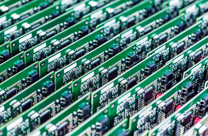
PCB fabrication is the process of manufacturing the bare board itself, the physical structure that will eventually carry all of your electronic components. At this stage, nothing is fitted. The output is a clean, structurally complete circuit board with conductive traces, drilled holes, and a solder mask applied, but no components in sight.
The Fabrication Process, Step by Step
Fabrication begins with your design files, most commonly a Gerber file set, along with drill files and a fabrication drawing. From there, the process follows a defined sequence:
- Substrate selection: The base material is chosen according to the application. FR-4 fibreglass-reinforced epoxy is the standard for most industrial and commercial designs. High-temperature laminates and PTFE-based materials are used where RF performance or elevated operating temperatures demand it.
- Copper lamination: Copper foil is bonded to the substrate to form conductive layers. Multilayer boards are built up by laminating multiple copper and dielectric layers together under heat and pressure.
- Etching: Unwanted copper is chemically removed, leaving behind only the conductive traces, pads, and planes defined in your design.
- Drilling: Holes are drilled for through-hole components and vias. Complex designs may use laser drilling for microvias in high-density interconnect (HDI) boards.
- Solder mask application: A protective layer is applied over the copper to prevent unintended solder bridges during assembly and to protect traces from oxidation.
- Silkscreen printing: Component reference designators, polarity markers, and other identification markings are printed onto the board surface to guide assembly.
- Bare board testing: The finished board undergoes electrical testing, typically flying probe or bed-of-nails, to verify that all traces are correctly connected and that no short circuits or open circuits are present.
What Fabrication Produces
The output of fabrication is a bare PCB: structurally complete, electrically verified, but entirely passive. It cannot do anything on its own. It is the foundation on which the next stage, assembly, builds a functioning circuit.
Board complexity at this stage is driven by layer count, minimum track and gap width, surface finish specification, impedance control requirements, and whether HDI techniques are needed. These decisions are made at the design stage and have a direct bearing on cost and lead time.
What Is PCB Assembly?
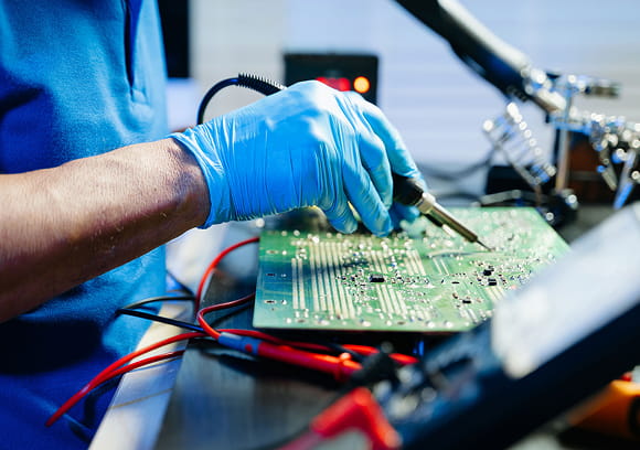
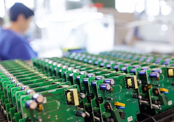
PCB assembly, often referred to as PCBA, is the process of mounting and soldering electronic components onto the fabricated board, transforming an inert structure into a working circuit. This is where resistors, capacitors, integrated circuits, connectors, and every other components are placed and permanently secured. You can see how we manage this end to end on our manufacturing process page.
Surface Mount vs. Through-Hole Assembly
The two principal assembly methods reflect the two main component package types in use today.
Surface Mount Technology (SMT) is the dominant method for modern electronic designs. A solder paste stencil is used to apply paste precisely to the component pads, an automated pick-and-place machine positions each component with high accuracy, and the populated board then passes through a reflow oven where the solder melts and forms permanent joints. SMT is well suited to compact, high-density designs and lends itself to full automation.
Through-hole assembly involves inserting component leads through drilled holes in the board. These are then soldered using either wave soldering, where the board passes over a flowing wave of molten solder, or selective soldering for mixed boards. Through-hole remains the preferred method for connectors, power components, and anything subject to significant mechanical stress.
Most real-world boards require both methods. A power supply board, for instance, might use SMT for the majority of its passive components but through-hole for its transformer, screw terminals, and heat-sunk devices. This mixed-technology build adds process steps and requires careful sequencing to avoid thermal damage to previously soldered components.
Inspection and Testing After Assembly
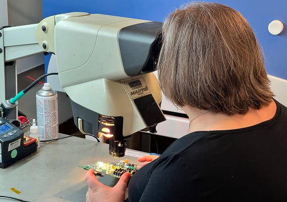
Assembly is not complete when the last component is soldered. For any application where reliability matters, a structured inspection and testing regime is essential.
- Automated Optical Inspection (AOI): Cameras scan the assembled board and compare it against the reference design, flagging missing, misaligned, or incorrectly oriented components.
- X-ray inspection: Used to examine solder joints that are hidden from view, particularly under Ball Grid Array (BGA) packages, where visual inspection is impossible.
- In-Circuit Testing (ICT): Probes test individual component values and connections across the board to verify that everything is present and correctly placed.
- Functional testing: The assembled board is powered up and tested under conditions that simulate real-world operation to confirm it performs as designed.
For products destined for defence, aerospace, or medical applications, this stage is not optional. It is the point at which conformance to the specified IPC class is formally verified.
How Both Stages Fit Into a Product Development Lifecycle
Understanding fabrication and assembly as isolated processes is useful, but what matters in practice is how they connect within the full journey from design to deliverable. A typical product development lifecycle looks like this:
- Concept and schematic design
- PCB layout and Design for Manufacturability (DfM) review
- Gerber and BOM file generation
- Fabrication of the bare board
- Component procurement
- Assembly (SMT, through-hole, or mixed technology)
- Inspection and testing (AOI, X-ray, ICT, functional)
- Box build and system integration where required
- Production scaling
The DfM review at stage two deserves particular attention. This is where a competent manufacturing partner will review the design and flag anything that could cause problems in fabrication or assembly, minimum clearances that are too tight for the process, component pad sizes that do not match the specified solder paste stencil, or via placements that will cause issues during wave soldering.
Identifying these issues before a board is fabricated is far cheaper than discovering them after.
Consider a practical example. An engineering team is developing a multilayer control board for an industrial automation system.
The board requires controlled impedance on several signal layers, a mixed-technology assembly with both SMT and through-hole components, and IPC Class 3 inspection throughout. If fabrication is sourced from one supplier and assembly from another, any discrepancy in DfM assumptions, stack-up interpretation, or quality class documentation becomes a problem that falls between two parties, with the customer caught in the middle.
A single partner responsible for both stages eliminates that interface entirely.
From Bare Board to Working Circuit
PCB fabrication builds the structure. PCB assembly creates the function. They are sequential, interdependent, and each demands specialist expertise, but they are not interchangeable, and treating them as such is a reliable route to avoidable problems.
For engineers working in defence, aerospace, medical, or industrial sectors, the stakes are higher than in consumer electronics. Quality class must be defined at the design stage. Testing cannot be an afterthought. And the choice of manufacturing partner matters as much as the quality of the design itself.
As PCB designs grow more complex, more layers, smaller components, tighter tolerances, more demanding environments, the integration of fabrication and assembly under a single, accountable supply chain becomes not just convenient but genuinely risk-reducing. Knowing that the same team who will assemble and test your board has already reviewed your design for manufacturability is a significant advantage when programme schedules and product reliability are on the line.
Every PCBA DSL produces also carries a 5-year warranty on all PCBAs, a direct reflection of the confidence we place in our processes.
If you are bringing a new design to production, or reviewing your current supply chain, get in touch with our electronic manufacturing team, we are ready to discuss your requirements, from initial design review through to full turnkey assembly and test.
Frequently Asked Questions
What is the difference between a PCB and a PCBA?
A PCB (Printed Circuit Board) is the bare, unpopulated board produced at the fabrication stage. A PCBA (Printed Circuit Board Assembly) is the completed board with all components soldered in place and ready for integration into a finished product.
Do I need different files for fabrication and assembly?
Yes. Fabrication requires a Gerber file set, drill files, and a fabrication drawing. Assembly additionally requires a Bill of Materials (BOM) and a component placement file (also called a Centroid or XY data file). Providing clean, accurate files for both stages from the outset avoids delays and costly queries later in the process.
Can I use separate suppliers for fabrication and assembly?
You can, but it introduces risk. Mismatched DfM assumptions, differing interpretations of IPC class requirements, and communication gaps between suppliers are a frequent source of rework and schedule slippage. A turnkey partner responsible for both stages removes that risk and provides a single point of accountability.
What IPC class does my product need?
This depends on your application. Class 2 covers most industrial and commercial electronics where consistent performance and extended life are required. Class 3 is required for defence, aerospace, and life-critical medical applications where failure cannot be tolerated. Critically, this decision must be made before design is finalised, a board fabricated to Class 2 cannot be upgraded to Class 3 after the fact.
How long does the full fabrication and assembly process take?
For standard-complexity boards, fabrication typically takes 3–7 working days and assembly a further 1–5 working days, depending on component availability, board complexity, and order volume. Working with a UK-based turnkey partner can reduce overall lead times by eliminating inter-supplier handoffs, international shipping, and incoming inspection delays at each stage.