 Your design passes every check in CAD. The schematic is signed off. Files go to your contract electronics manufacturer. Then the call comes: there is an issue. Maybe it surfaces at first inspection. Maybe in pre-production testing. Sometimes it appears months later, in the field, after your customer has already integrated your board into their own product.
The frustrating part is that these issues are predictable. The same common PCB design issues appear on incoming designs across the industry, year after year.
So if these problems are well known, why do they keep reaching production? The answer has more to do with how most contract manufacturers operate than with how engineers design. This article walks through the PCB design issues we see most often, why the standard CEM model lets them slip through, and what catching them earlier actually looks like.
Why design issues reach production in the first place
Most contract electronics manufacturers operate a gatekeeping model. You submit your design files. They run automated checks. They flag any issues. Then you face a choice: pay engineering charges to have their team resolve the problems, or take the design back, fix it yourself, and resubmit. Either route adds time and cost.
On top of that, most CEMs charge non-recurring engineering (NRE) fees to set up production for a new product, which can run into thousands of pounds before a single board is built. The commercial structure rewards finding problems late, not early.
There is also a technical gap that gets overlooked. A Design Rule Check (DRC) confirms your design follows the rules you set in your CAD tool. A Design for Manufacturability (DFM) check confirms it can actually be built using the chosen factory’s specific equipment, materials and process windows. A board can pass DRC and still fail DFM. The two are not the same.
The deeper issue is the difference between a CEM that interprets your data and one that designs alongside you. Most contract manufacturers receive your Gerbers, run them through CAM software, and react to what the software flags. Few have on-site design engineers who design complex boards themselves. That distinction matters because experienced designers recognise issues that automated checks can sometimes miss.
Industry studies suggest 70 to 80% of product cost is locked in at the design stage. Yet manufacturer involvement typically begins after the design is finished. By then, fixing a fundamental issue means redesign, not mere adjustment.
The PCB design issues we see most often
These cluster into five recurring problem areas. All are preventable.
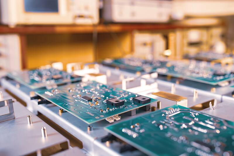
1. Footprint and library errors
Most CAD tools include libraries of common components with verified footprints. Problems start when designers use parts that are not in the library, or rely on outdated library data that no longer matches current manufacturer part numbers.
A custom footprint with pad spacing off by half a millimetre will not solder correctly. A 0402 resistor with mismatched pad dimensions will tombstone during reflow, standing on end with one terminal lifted. Fine-pitch ICs with incorrect land patterns will not align to their pads at all.
These issues rarely show up in DRC because the rules are checking against your library, not against reality. They get caught at first article inspection or, worse, during functional test on a fully assembled board.
2. Components designed in at end of life or NRND
Component obsolescence has accelerated sharply.
Over 30% of electronic components become obsolete within five years of introduction, and 2026 is bringing additional pressure on mature-node semiconductors as foundries shift capacity toward leading-edge production.
When an end-of-life or not-recommended-for-new-design (NRND) component gets specified at design stage, the consequences cascade. You may need to forward buy stock to cover production, hurting cash flow. You may face last-minute substitutions that introduce subtle electrical differences. For regulated sectors, a component change can trigger requalification or even full recertification.
This is one of the strongest cases for involving design engineers, not just CAM operators, in early review. Recognising lifecycle risk on a BOM requires someone who understands the components themselves, not just the design files. DSL’s in-house design engineers flag at-risk parts before they become a sourcing emergency.
3. Manufacturability faults that pass DRC
This is where the DRC versus DFM distinction matters most. Your design passes every rule check, but the board still cannot be reliably manufactured. Common offenders include:
- Acid traps. Acute angles where traces meet pads cause etchant to pool during fabrication. The trapped acid over-etches nearby copper, creating openings or trace necking. Keeping trace approach angles at 45 or 90 degrees prevents this.
- Slivers and islands. Free-floating copper fragments on plane layers can detach during the etching process, drift across the panel, and create shorts on adjacent boards. Larger islands act as antennas, introducing noise.
- Insufficient annular rings. When the copper ring around a drilled hole is too thin, drill drift during manufacturing can cause breakout, leaving an unreliable connection.
- Asymmetric layer stack-ups. Unbalanced copper distribution across layers is one of the leading causes of warpage in multilayer boards.
DRC misses these because the rules in your design tool do not match the factory’s actual process windows. A proper PCB DFM check compares your design against what the factory can actually build, not against generic IPC defaults.
4. Solder joints hidden from inspection
A board can be assembled correctly and still ship with defects nobody can see. When component placement creates shadows, or when tall components sit next to small passives, automated inspection systems lose visibility on critical solder joints.
This is a design issue, not a manufacturing one. The decision to place a connector next to a fine-pitch BGA might have been driven by signal integrity, but if it makes the BGA’s joints invisible to inspection, you have created a field failure waiting to happen. The board will pass first article. It will pass functional test. Then a thermal cycle in the field will fracture a marginal joint nobody knew existed.
This is why every board DSL produces goes through 3D AOI inspection, and why design choices that make joints invisible to inspection get flagged before production starts.
5. Documentation gaps
Even a perfectly designed board can stall in production because of incomplete documentation. Missing layer files, ambiguous BOMs without manufacturer part numbers, no DNP (do not populate) notes, or contradictions between drill files and Gerber data all force the manufacturer to either pause and ask questions, or build to assumption.
Documentation issues typically add 2 to 4 days to production just for issue resolution. Neither outcome is good for an OEM working to a tight launch window.
The frustrating truth is that documentation gaps take 30 minutes to fix at design stage and become genuinely difficult to resolve once production has started. They also strongly suggest that design teams and manufacturing partners are not communicating early enough.
How DSL approaches common PCB design issues differently
Most CEMs review your data. DSL’s on-site design engineers design complex PCBs every day, which is why they spot issues that automated checks can miss. That difference shapes the entire engagement model.
The Design Health Check is offered before commitment, not as a paid gate after submission. The Re-design service tackles existing products that have inherited issues from previous manufacturers, including obsolete components, unnecessarily high unit costs, and reliability problems baked in years ago.
There is no NRE on any project. DSL absorbs the setup costs (programming pick-and-place machines, creating solder stencils, configuring AOI inspection profiles, building test fixtures) because catching design issues early and getting a board right first time is part of how DSL builds, not an extra service.
Every board passes through 3D AOI on the fully automated SMT line, every time. The 5-year warranty on every PCBA is the consequence of this process discipline, not a marketing layer added on top.
What good design-stage collaboration actually looks like
A PCB design review that genuinely catches the most common PCB design issues looks different from a CAM-software pass. It includes:
- Schematic stage involvement, not Gerber stage submission. By the time files are ready for fabrication, fixing major issues means redesign.
- BOM review for component lifecycle, not just current availability.
- Footprint validation against the manufacturer’s actual library, not a generic IPC reference.
- Stack-up confirmation before final layer assignment, particularly for multilayer boards.
- Inspection access review, ensuring 3D AOI can see every critical joint.
- Documentation pack review before fabrication submission.
This is how every project should run. Most do not, because the standard commercial model puts a charge on every conversation.
Catching the issues that matter, before production
The most common PCB design issues are not exotic. They are footprint errors, end-of-life components, DRC-passing manufacturability faults, hidden solder joints and incomplete documentation. They appear on the majority of incoming designs because the standard CEM model rewards finding them late, not because designers are careless.
A different model exists. One where design engineers work with your data from the schematic stage. One where reviewing your design does not come with a charge attached. One where every board is inspected with 3D AOI as standard, and where the warranty is five years because the process supports it.
The result is fewer respins, faster lead times, better yields and a board that works first time. If you want a second pair of expert eyes on your design before it goes into production, book a Design Health Check with our team.
FAQs
What is the difference between a DRC and a DFM check?
A DRC confirms your design follows the rules you set in your CAD tool. A DFM check confirms it can actually be built by the chosen factory using their specific equipment, materials and process windows. A board can pass DRC and fail DFM.
Why do PCB design issues keep reaching production?
Because most contract electronics manufacturers only review designs after submission, often with charges attached to fix what they find. Engineers naturally avoid early reviews when each one comes with a fee. Removing that commercial barrier changes when issues get caught.
How early should a manufacturer be involved in PCB design?
At schematic stage, not at Gerber submission. By the time files are ready for fabrication, fixing major issues means redesign rather than adjustment.
What does a Design Health Check actually cover?
Footprint accuracy, component lifecycle status, manufacturability against actual factory capability, inspection access, stack-up balance, and documentation completeness. The aim is to catch every issue that would otherwise surface during production.
Are PCB design issues only a problem for inexperienced designers?
No. Industry data shows that over 30% of all incoming designs have issues, including from highly experienced teams. The pattern is consistent across company size and designer seniority because the issues are systemic, not skill-based.